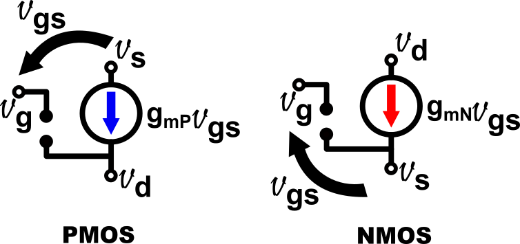
Small signal model is an atttempt to obtain linear model of the MOSFET by only focusing on the small deviations. From the previous section, we can see that under small signal assumptions, the role of the MOSFET is to induce \(i(t)\) which is proportional to the input signal \(v_{GS}(t)\). This means that when focusing only on the small deviations, MOSFET is equivalent to a linear voltage controlled current source as shown in Fig.6.

now let us recall from the previous section that the slope \(g_{mP} \) is negative ( \(g_{mP} \le 0 \) ). Denoting \(g_{m}=g_{mN}=-g_{mP} \), we obtain the same equivalent circuit for both PMOS and NMOS shown in Fig.7.

As sanity check, let us solve for signal gain in the previous example by subtituting the transistors with the model. In both NMOS and PMOS case, the small signal equivalent circuit of the previous example is as shown in Fig.7 below.

Applying kirchoff current law at the node \(v_{d} \) we get \[ g_mv_{GS}(t) +\frac{v_{DS}(t)}{R}=0 \Rightarrow \frac{v_{DS}(t)}{v_{GS}(t)}=-g_mR\] We indeed obtain the same result as the previous section.
To summarize, MOSFET devices can be modeled as linear current source during small signal operations. By modeling the transistor with linear current source, the calculation of the circuit can be simplified significantly.