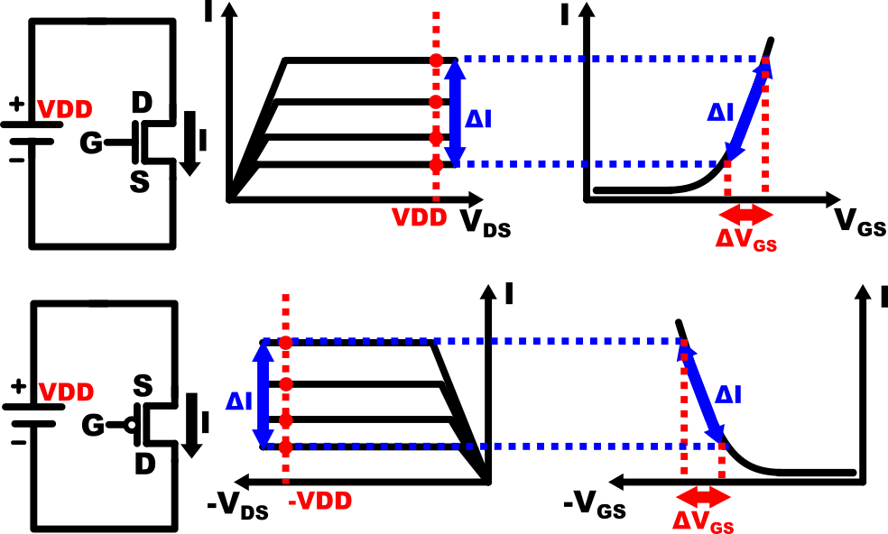
The goal of this section is to illustrate the intuition behind how voltage amplification is performed in a simple circuit using MOSFET. In this particular example, we aim to achieve voltage amplification from the gate(G) to the drain(D) terminal of the MOSFET.

Let's start by connecting the drain and source terminal of NMOS and PMOS directly to a battery with voltage value VDD. When VDD is chosen properly such that it exceeds \( V_{saturation}\) , the operation of the MOSFETs are summarized in Fig.3. Since the voltage at the source(S) terminal is constant, some change in gate voltage \( \Delta V_{G}\) will directly induce change in the value of \( V_{GS}\) \( ( \Delta V_{GS} )\). \(\Delta V_{GS} \) will in turn induce change in the flowing current value\( (\Delta I )\) as shown in the figure above. This result shows that \( \Delta V_{G}\) can in fact affect the amount of current flowing through the device by \( \Delta I \)
With the circuit as is however, although \( \Delta I \) exists, it cannot be converted to change in drain voltage \( \Delta V_{D}\) or \( \Delta V_{DS}\). This is because currently the drain and source is connected to the battery, hence their relative value will remain at VDD regardless of the flowing current (obviously). So, how can we capitalize on this \( \Delta I \) to realize voltage amplification? let's try adding a resistor in series to the drain terminal like in Fig.4 below*.
* This structure is commonly known as common-source amplifier

By loading the MOSFET, the voltage at drain terminal (\( V_{D} \)) is now affected by the voltage drop of the resistor which is proportional to the flowing current (by ohm's law). For the sake of simplicity, in this example the size of R is chosen properly such that the MOSFET remains in saturation in regardless of the change in (\( V_{D} \)) as shown in Fig.4. Solving for \( V_{DS} \) and drain voltage (\( V_{D} \)) of each transistor, we get:
- for PMOS: \( V_{DS}= - (VDD-IR) \Rightarrow V_{D}=IR \), hence \( \Delta V_{D}=\Delta IR \)
- for NMOS: \( V_{DS}= VDD-IR \Rightarrow V_{D}=VDD-IR\), hence* \( \Delta V_{D}=-\Delta IR \)
* since VDD is constant
From the equations, we can confirm that the value of \( V_{DS} \), and therefore \( V_{D} \) in both cases change as the current changes. Therefore, from this result, we can conclude that voltage amplification from \( V_{G} \) to \( V_{D} \) can indeed be realized in this circuit using the chain reaction shown below. \[ \Delta V_{G} \rightarrow \Delta V_{GS} \rightarrow \Delta I \rightarrow \Delta V_{DS} \rightarrow \Delta V_{D}\]Calculating this voltage amplification effect quantitatively usually is no easy feat. Although we can do it for the previous example if we try, in more complicated circuits, the problem gets difficult really fast. The difficulty mainly arise from the fact that the relationship between \( \Delta V_{GS} \) and \( \Delta I \) is often non-linear and the fact that the transistor can fall out of saturation* when its voltages change too much.
* when not in saturation, the flowing current will change depending on the voltage. This current change may affect other components in more complicated circuits
In practice, we often use approximations to perform the calculation which can greatly reduce the difficulty of the problem. One of the approximations is small signal analysis which will be explained in the next section.