In this article we are going to discuss two important practical considerations that must be taken into account during the design of a charge pump; clock frequency consideration and voltage control loop consideration.
Clock Frequency Consideration
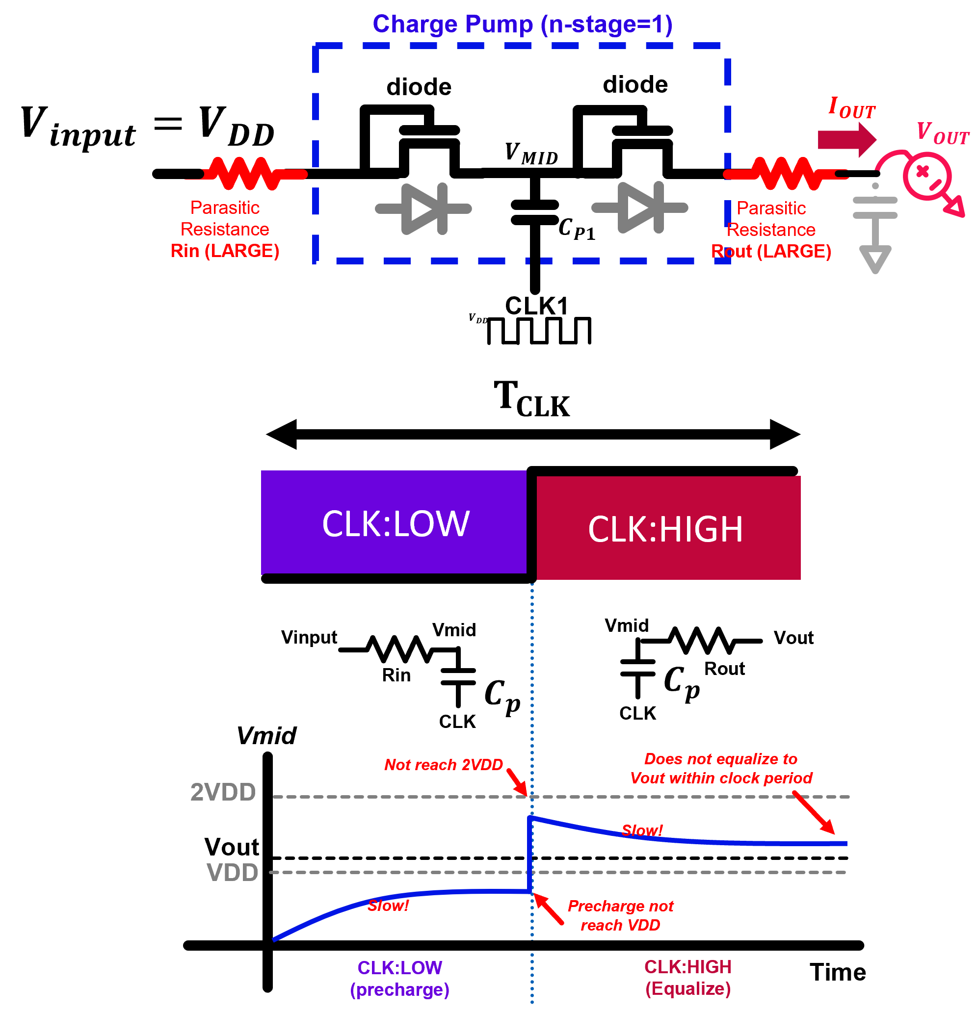
This consideration mainly covers the relationship between pump clock frequency, pump capacitance and routing resistances. Since the output current of a charge pump is expressed as \( I_{OUT-AVG}=\frac{\Delta Charge}{T_{CLK}} \), it can be improved by reducing \( {T_{CLK}} \) . However, in the real world, we cannot reduce \( {T_{CLK}} \) indefinitely since charge equalization and precharge process do not happen instantaneously. The time required for pre-charge operation and charge equalization operation to complete is decided by RC delay due to the value of pump capacitance \(C_{p}\) and the value of parasitic routing resistances inside the charge pump,\(R_{IN}\) and \(R_{OUT}\). If \( {T_{CLK}} \) is too short (or RC delay is too big), there won't be enough time during precharge and equalization operation. This will degrade output current of the charge pump as shown in Figure 1 below.

As a rule of thumb, it is adivsable to keep pump clock period above 4-5 times \(RC_{p}\) such that around 90% of the charge is transferred from/to \(C_{p}\) at each clock transition. For example, when Tclk is chosen to be around 4RC, precharge and equalization each has around 2RC to complete their operation. Since \(e^{-\frac{2RC}{RC}} \approx 0.13\), this means that around 87% of the charge is transferred during precharge and equalization operation. \[ T_{CLK} \geq 4 \sim 5 \times MAX(R_{IN},R_{OUT}) \times C_{p} \] On top of this, one can also adjust the duty cycle of the clock signal such that the alloted time for precharge and equalization is different within one clock cycle. For example, with Tclk=4RC, if we know that Rin is very small (fast precharge), but Rout is large (slow equalization), we can prepare 75% duty cycle clock signal such that 1RC is alloted for the fast precharge and 3RC is alloted for the slow equalization process. It should be mentioned however, that the control for such scheme might become complicated if we have multiple charge pumps connected in parallel.
Voltage Control Consideration (Feedback Loop)
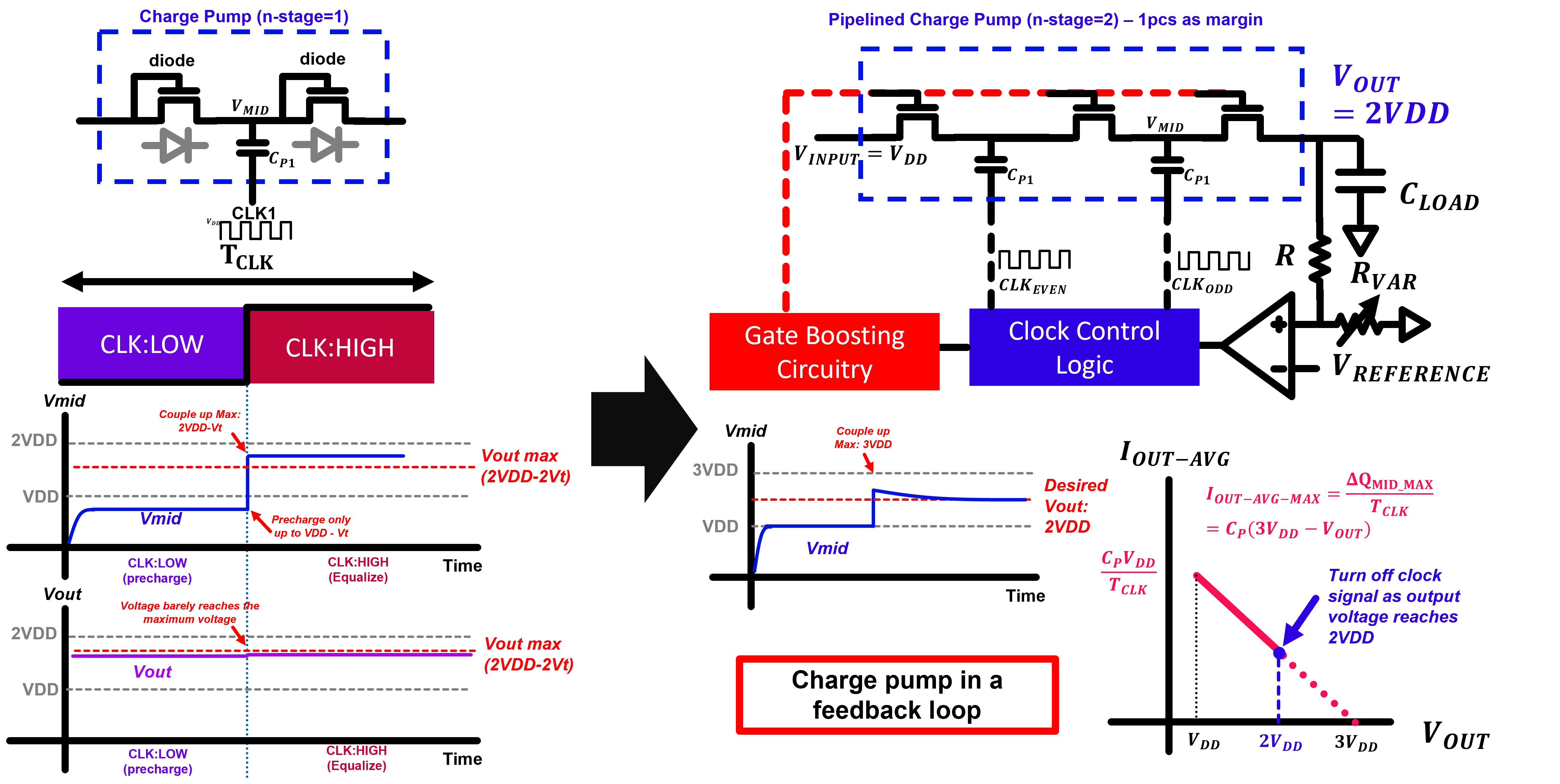
As mentioned in the previous chapters, the output current of charge pump decreases as its output voltage increases. This means that it might take a very long time for a charge pump to reach the desired target voltage of 2VDD. Furthermore, diodes in the charge pump might have non-zero threshold voltage (Vt) which will decrease the final reachable voltage to 2VDD-2Vt in our 1-stage charge pump example. The threshold voltage Vt might also vary due to process variation which leads to some variance in the output voltage. To account for all these problems, charge pump is usually implemented as a part of voltage control loop shown in Figure 2 below.

The voltage control loop consists of charge pump, voltage comparator, clock control logic, and gate boosting circuitry. The charge pump consists of more stages than necessary to make sure that sufficient output current can be produced even as the output voltage increases, which will lead to faster response. The voltage comparator consists of voltage divider and amplifier. The output of voltage comparator controls the "enable" signal for clock control logic. When the divided output voltage is lower than \(V_{REFERENCE}\), clock signal is activated and pumping mechanism starts. On the other hand, when the divided output voltage is larger than \(V_{REFERENCE}\), clock signal is turned off and pumping mechanism stops. The clock control logic also controls gain boosting circuitry. The gain boosting circuitry is required so that transistor's Vt does not hinder charge pumping mechanism. It provides proper high voltage to the gate of transistors that need to be turned on during operation. All in all, when the voltage control loop works properly, the output voltage can be expressed by the equation below: \[ V_{OUT}=\frac{R_{VAR}+R}{R_{VAR}} \times V_{REFERENCE} \]
As shown in the equation above, we can control the final value of \(V_{OUT}\) by tuning the value of \(R_{VAR}\) . We have to remember here that although \(V_{input}=V_{DD}\) is no longer included in the equation for \(V_{OUT}\), it still plays an important role in the voltage control loop. This is because voltage range that can be produced by the loop is decided by the value of \(V_{input}\) . If \(V_{input}\) is made too low or number of pump stages are made too few, \(V_{out}\) will not be able to be generated properly, no matter how we tune \(R_{VAR}\) and \(R\).
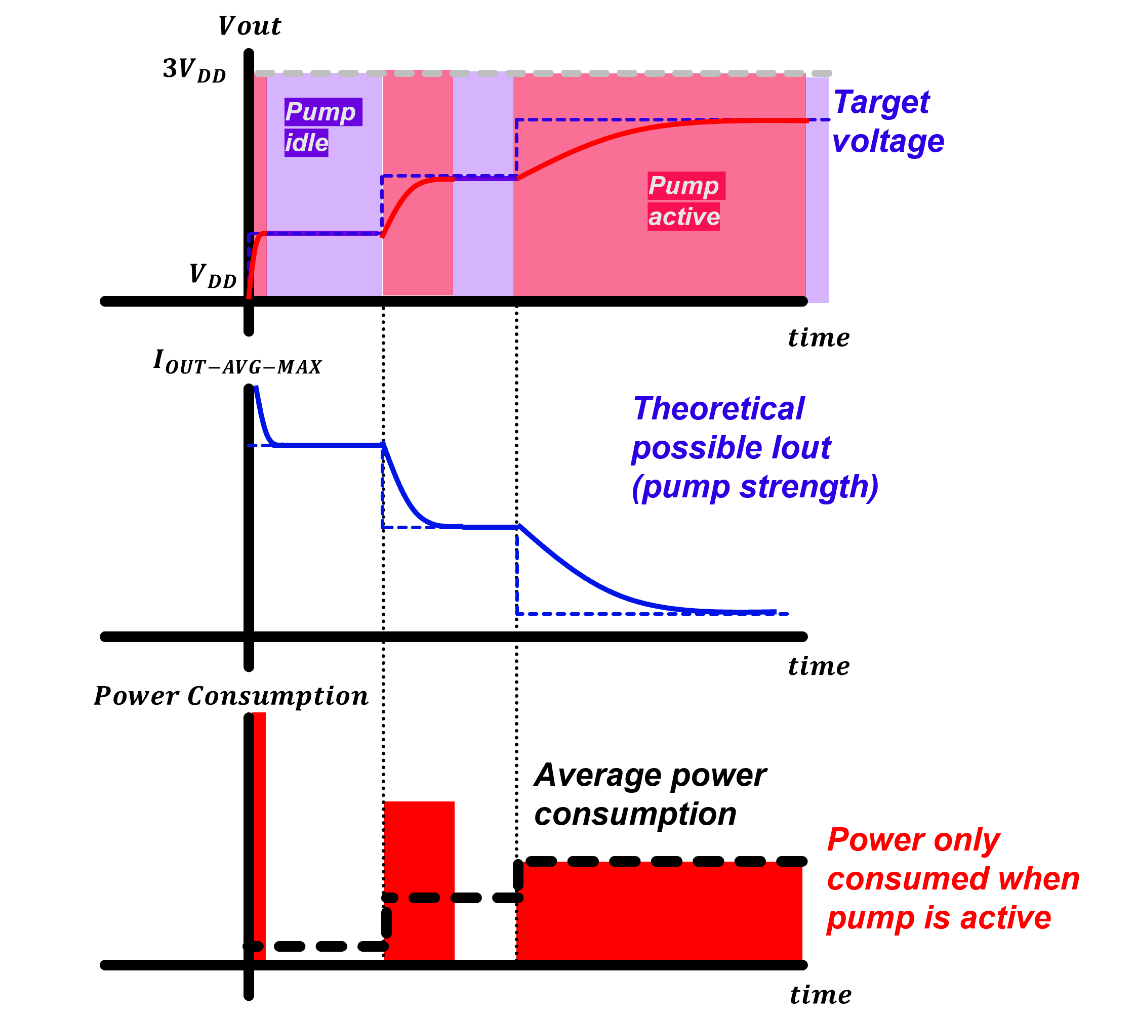
Another interesting fact about voltage control loop is its power consumption. One might think intuitively that larger pump strength (in lower voltage region) will lead to higher power consumption. While this might be true for instantaneous "peak" power, it might not be the case for average power consumption. The Figure 3 below shows an example of such case.

If we set the target voltage to progressively higher value step by step as shown in the figure above, despite higher peak power consumption at lower voltage levels due to larger pump strength, the average power consumption of the whole loop at lower voltage can be lower compared to average power consumption at higher output voltage levels. This is because the feedback mechanism turns the pump off after output voltage reaches the desired target voltage, resulting in longer "pump idle" period at lower voltages. On the other hand, in higher output voltage levels, although pump strength is weaker, the pump must be active for longer period before achieving the desired level which can result in increase in overall average power consumption of the whole voltage control loop.