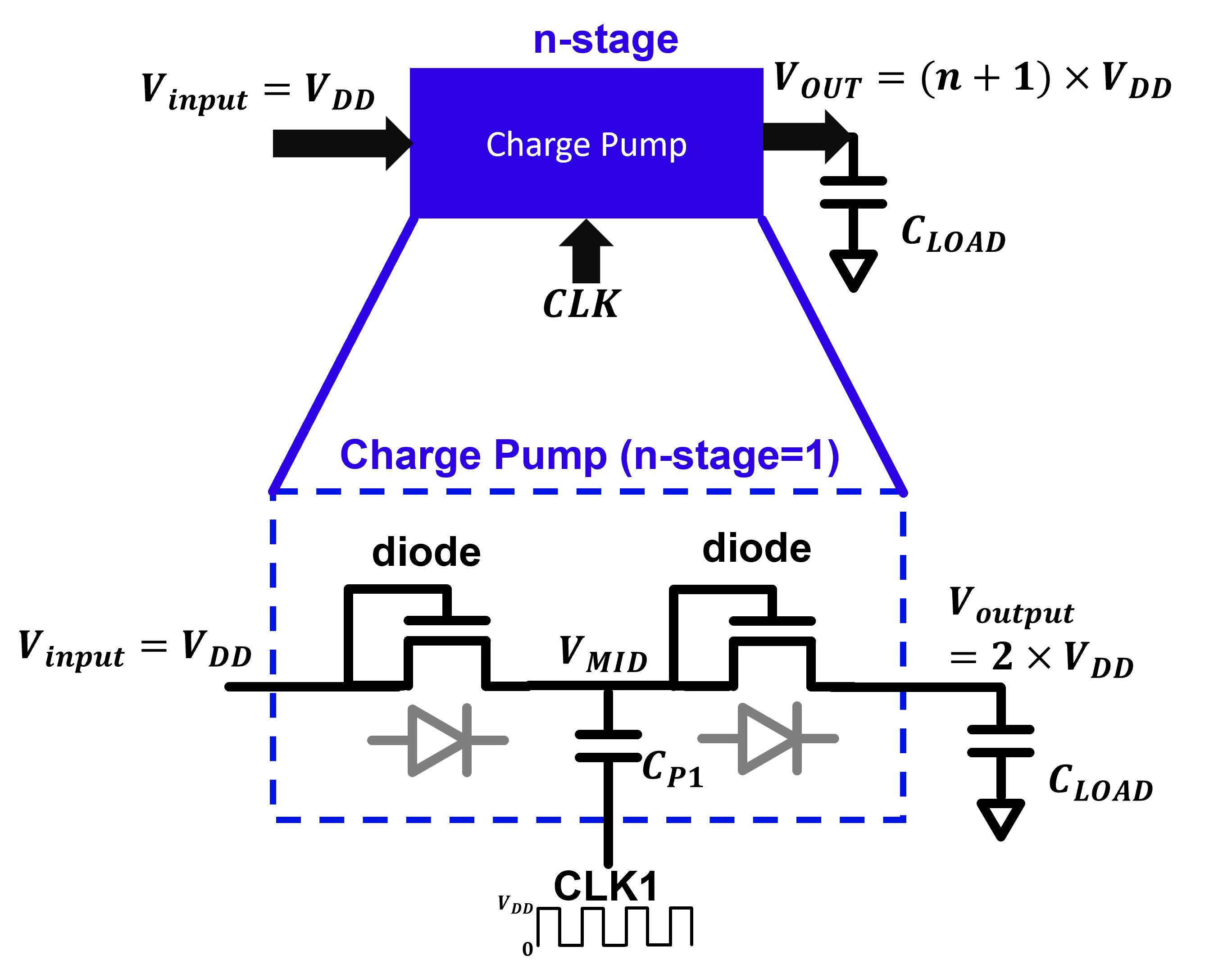
Charge pump is a voltage generation circuit that utilizes the accumulation and transfer of electric charge to produce higher voltage levels within electronic devices. It is commonly employed in integrated circuits to provide the necessary voltages for powering components, eliminating the need for multiple external voltage inputs. Unlike switching regulators, charge pumps can generate higher voltages without using any inductors, making it compact, efficient, and easily integrated. Due to these advantages, charge pump is vital for modern electronics, offering a space-efficient solution for regulated voltage level generation.
General concept of a charge pump and its typical implementation with Dickson type charge pump is shown in Figure 1. A charge pump takes arbitrary supply voltage as input and outputs a certain multiple of the input voltage. Typically, the higher the desired output voltage, the more the required number of stages in a charge pump. In the dickson type implementation, a charge pump stage consists of two diodes and a capacitor. One node of the capacitor is connected to both diodes, while the other node is connected to a CLK signal as shown in the figure. The dynamics provided by this capacitor and the clock signal is key to the operation of the charge pump.
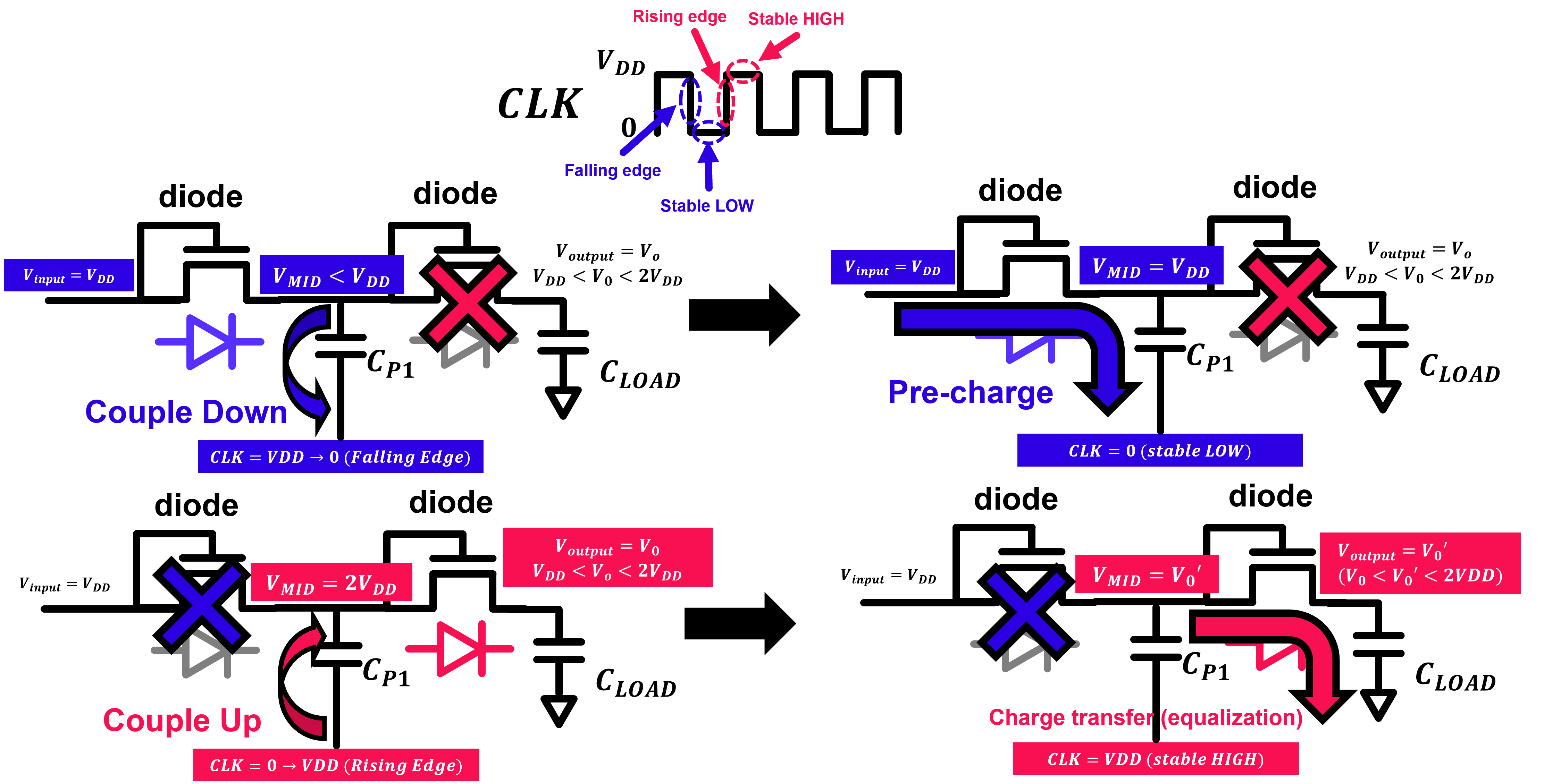
Figure 2 shows the charge pump operation at each CLK signal state. When CLK is at falling edge ( \(CLK: V_{DD} \rightarrow 0\) ), the voltage at node \(V_{MID}\) is coupled down to a voltage lower than \(V_{DD}\). Then, during CLK=LOW period, the \(V_{MID}\) voltage is precharged to \(V_{DD}\). During these CLK=LOW periods, the input diode (left side) is at ON state, while the output diode (right side) is at OFF state (cut off). On the other hand, When the CLK is at rising edge ( \(CLK: 0 \rightarrow V_{DD}\) ), the voltage at node \(V_{MID}\) is coupled up to \(2V_{DD}\). Then, during CLK=HIGH period, the \(V_{MID}\) voltage is equalized with \(V_{OUT}\) such that both voltages become \(V_{O}'\) ( i.e. \(V_{MID}=V_{OUT}=V_{O}'\) ). During these CLK=HIGH periods, the input diode (left side) is at OFF state, while the output diode (right side) is at ON state.
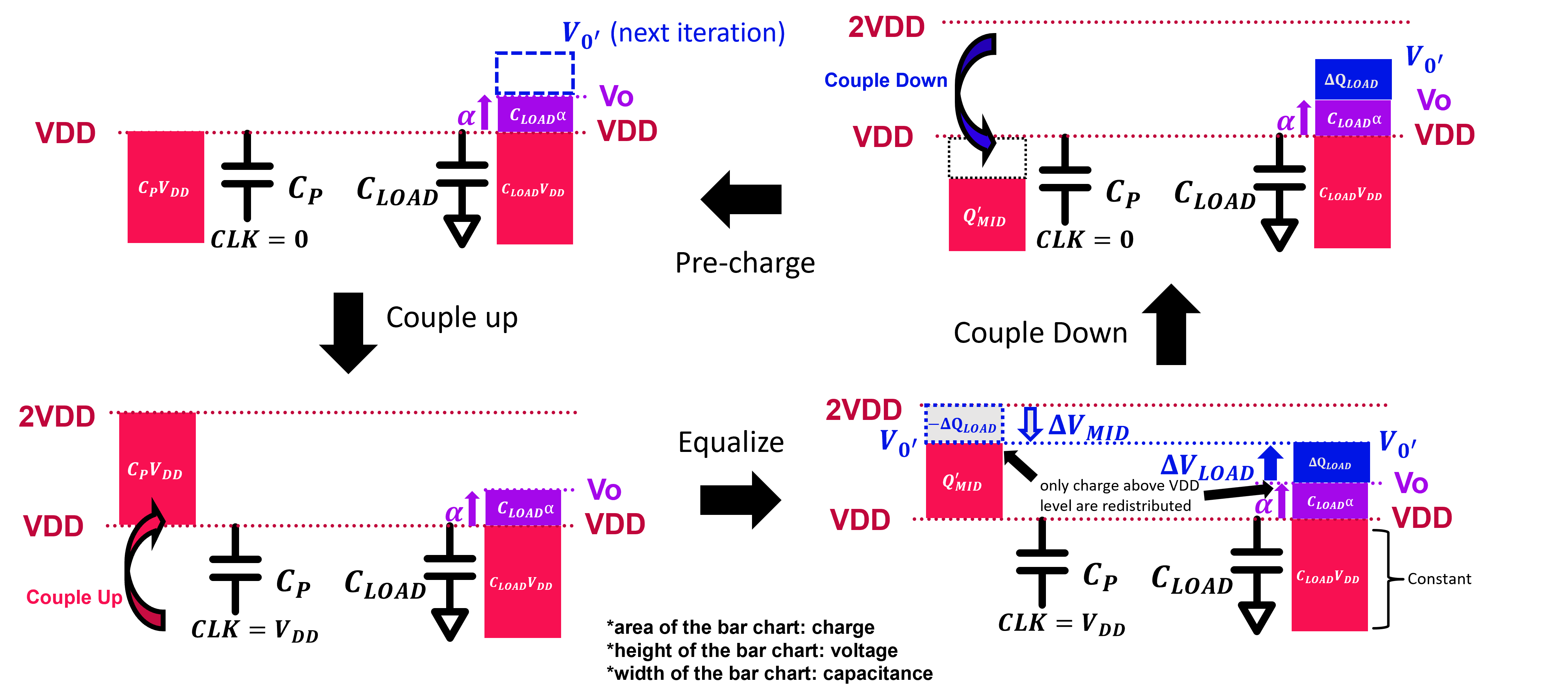
Figure 3 shows charge transfer diagram between pump capacitor and load capacitor. The width of the bar charts represent the capacitance of each capacitor, the height of the bar charts represent the voltage of each capacitor and the area of the bar chart represents the amount of charge stored in each capacitor. In the diagram, excess voltage over VDD at the output node is represented by the quantity \( \alpha \) . From the diagram, we see that pumping mechanism at each clock cycle can be separated into 4 different operations as follows:
- Pre-Charge This operation happens during CLK=LOW period. In this state, pump capacitor is precharged by the input until its top node's voltage reaches \(V_{DD}\). There is no change in charge state at load capacitor. After the pre-charge operation is complete, charge at pump capacitor and load capacitor are expressed by the equations below: \[ Q_{MID0}=C_{p} \times (V_{input}-CLK) = C_{p} \times (V_{DD}-0) = C_{p}V_{DD} \] \[ Q_{LOAD0}=C_{LOAD} \times (V_{out}-0) = C_{LOAD}V_{0} \]
- Couple-Up This operation happens when CLK signal transitions from LOW to HIGH ( \(CLK: 0 \rightarrow V_{DD}\) ). One important concept to consider here is that during this operation, there is no change in the amount of stored charge inside the capacitors. The couple-up operation merely shifts the voltages between the nodes of pump capacitors without changing the amount of charge stored in it. As the result, \(V_{MID}\) is pushed to 2VDD by the movement of the CLK signal as shown below: \[ Q_{MID}=Q_{MID0} \] \[C_{p} \times (V_{MID}- CLK) = Q_{MID0} \] \[C_{p} \times (V_{MID}- V_{DD}) = C_{p}V_{DD} \] \[\rightarrow V_{MID} = 2V_{DD} \]
- Equalization This operation happens during CLK=HIGH and is the most important step in charge pumping mechanism. During this period, charge from pump capacitor is transferred to load capacitor. The most important thing to realize here is that not all charge in \(C_{p}\) is transferred to \(C_{LOAD}\) . The charge is only redistributed until voltages at both capacitors become equal ( i.e. \(V_{MID}=V_{OUT}=V_{0}'\) ), at which point there is no more current flowing between the two capacitors. \(\Delta Q_{LOAD}\) shows the amount of charge transferred from \(C_{p}\) to \(C_{LOAD}\). The fact that all of the charge that left \(C_{p}\) must go to \(C_{LOAD}\) implies voltage movements at each capacitor are not the same and will depend on capacitance value of each capacitor ( \(\Delta V_{MID} \neq \Delta V_{OUT}\) ). Final voltage after equalization, \(V_{0}'\) and the amount of transferred charge, \(\Delta Q_{LOAD}\) can be calculated as follows: \[ Condition1: Voltage \space Equalization \Rightarrow V_{MID}=V_{OUT}=V_{0}' \] \[ Condition2: Charge \space Conservation \Rightarrow Q_{MID}'+Q_{LOAD}'=Q_{MID0}'+Q_{LOAD0}' \] \[ \Downarrow \] \[ C_{p} (V_{0}'-CLK) + C_{LOAD} (V_{0}') = C_{p}V_{DD} + C_{LOAD}V_{0} \] \[ C_{p} (V_{0}'-V_{DD}) + C_{LOAD} (V_{0}') = C_{p}V_{DD} + C_{LOAD}V_{0} \] \[ V_{0}' = 2V_{DD}\frac{C_{p}}{C_{p}+C_{LOAD}} + V_{0}\frac{C_{LOAD}}{C_{p}+C_{LOAD}} \] \[ \Delta Q_{LOAD} = Q_{LOAD}'-Q_{LOAD0} = C_{LOAD}V_{0}'- C_{LOAD}V_{0}\] \[ \Delta Q_{LOAD} = ( 2V_{DD}-V_{0} )\frac{C_{p}}{C_{p}+C_{LOAD}} \] Here, we see a very interesting behavior. The amount of transferred charge \(\Delta Q_{LOAD}\) decreases as the value of output voltage ( \(V_{OUT}=V_{0}\) ) increases. The amount of transferred charge ultimately approaches 0 as \(V_{OUT}\) approaches \(V_{OUT}=2V_{DD}\). This behavior puts a theoretical limit on the amount of maximum current a charge pump can provide to its load which will be explained further in the next chapter.
- Couple-Down This operation happens when CLK signal transitions from HIGH to LOW ( \(CLK: V_{DD} \rightarrow 0\) ). Same as couple-up, in the couple-down operation there is no change in the amount of stored charge inside the capacitors. The couple-down operation simply shifts voltages between the nodes of pump capacitors without changing the amount of charge stored in it. Since some of its initial charge has been transferred to \(C_{LOAD}\) during equalization, \(V_{MID}\) is pulled to a voltage level lower than VDD by the movement of the CLK signal during the couple-down operation. The couple-down operation completes the pump cycle and sets the initial state for precharge operation of the next iteration.
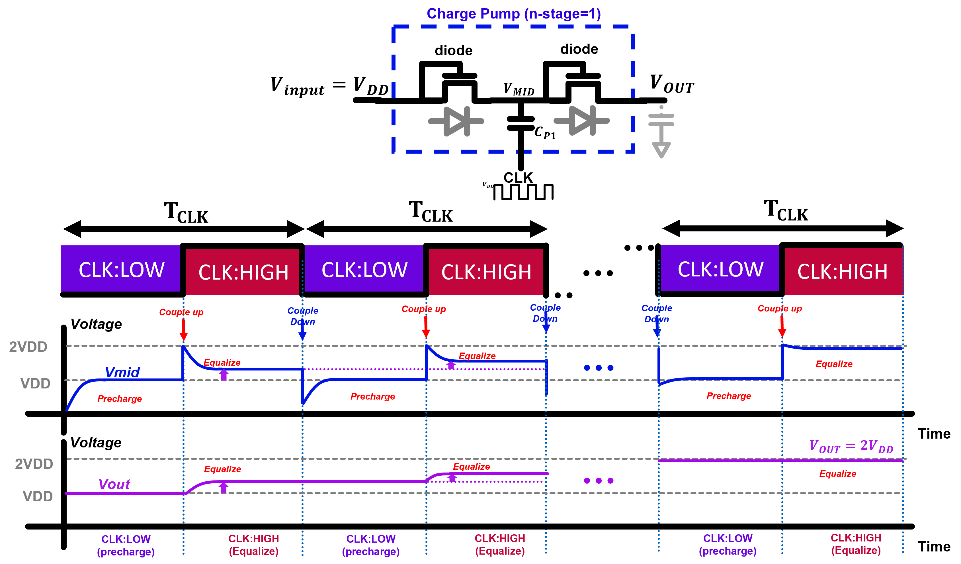
By repeating 4-step mechanism mentioned previously over multiple clock cycles, higher voltage at the output node can be generated. Figure 4 below shows waveform of typical charge pump operation. The output voltage rises step by step to the desired voltage of 2VDD with each clock cycle iteration. During the first few iterations when the output voltage is still far from 2VDD, we can see big Vout voltage jumps at each iteration since large amount of charge can be transferred to load capacitor at each couple-up operation. However, as the output voltage approaches 2VDD in later iterations, we can see that the voltage jumps are getting smaller since only a small amount of charge can be transferred to the load at each iteration.
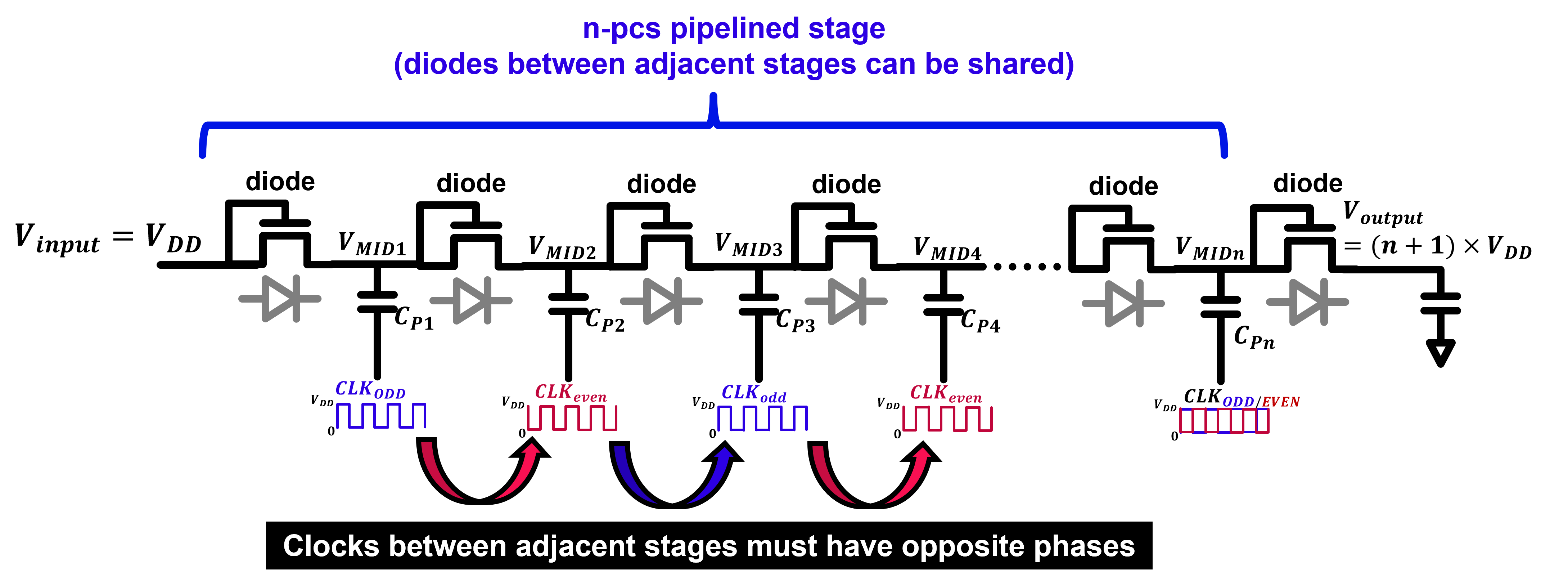
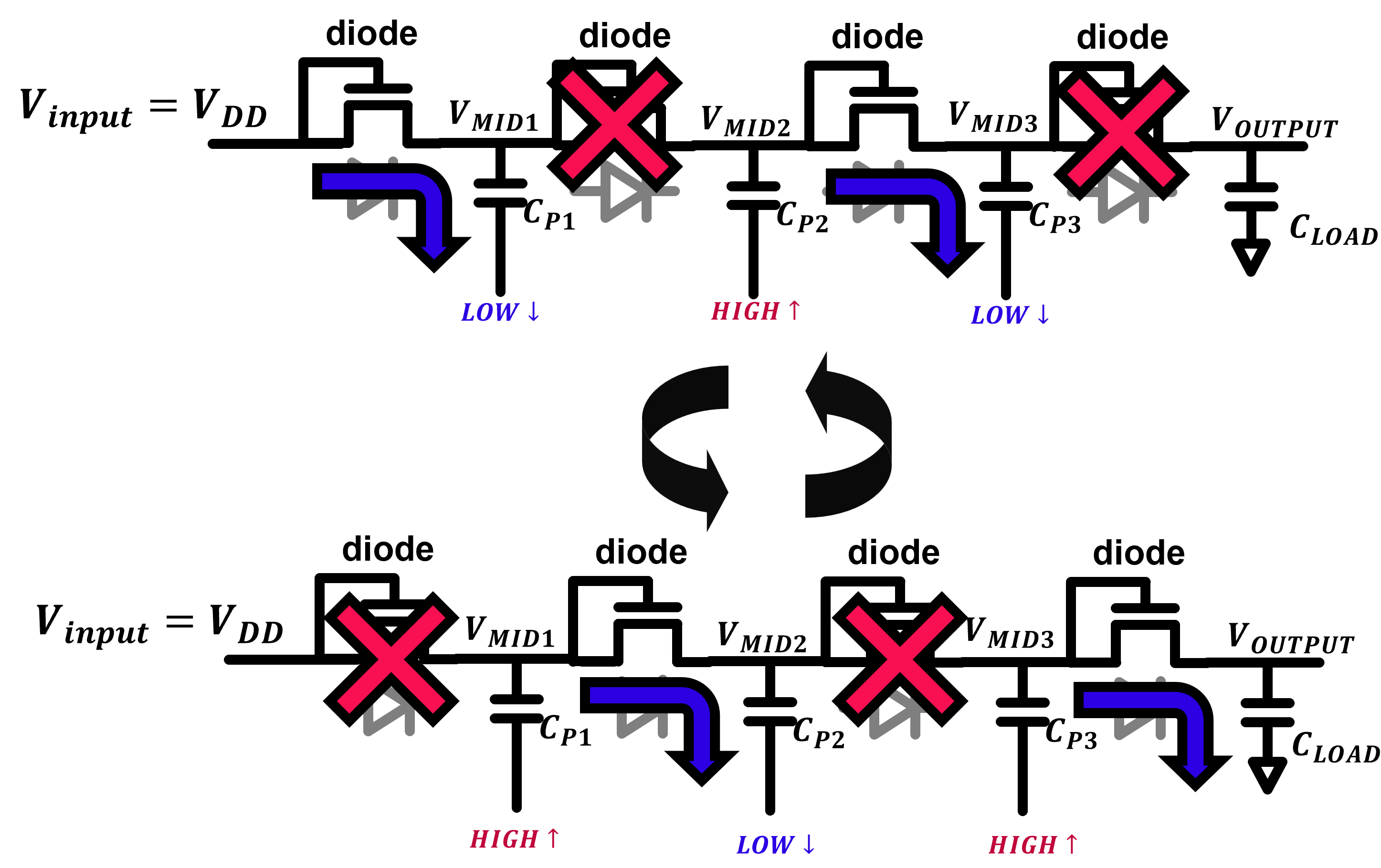
To generate higher voltages, indeed we can simply cascade multiple pump stages explained before such that the output voltage becomes \(V_{OUT}=(n+1)V_{DD}\) , where n is the number of cascaded stages. However, we can further reduce the amount of required transistors by pipelining multiple charge pump stages as shown in Figure 5 below. In pipelined configuration, one diode between two adjacent stages can be removed, hence reducing the number of components while maintaining same pump functionality. In this configuration, clock signal between two adjacent stages must have opposite phases such that when one stage is performing precharge operation, the other is performing equalization operation as shown in Figure 6.
In conclusion, charge pump provides area-efficient solution to on-chip voltage generation problem. Unlike switching regulators, it does not require any inductors to generate higher voltages, making it easier to implement in various chips. Charge pump typically consists of multiple stages. The number of stages in a charge pumps directly correlates to the charge pump's maximum outputtable voltage. Inside each stage, higher voltage is generated by the dynamics provided by the clock signal and pump capacitor. To generate higher output voltage while reducing overall required components, we can put charge pump stages in pipeline configuration where extra diode between two adjacent stages can be removed.